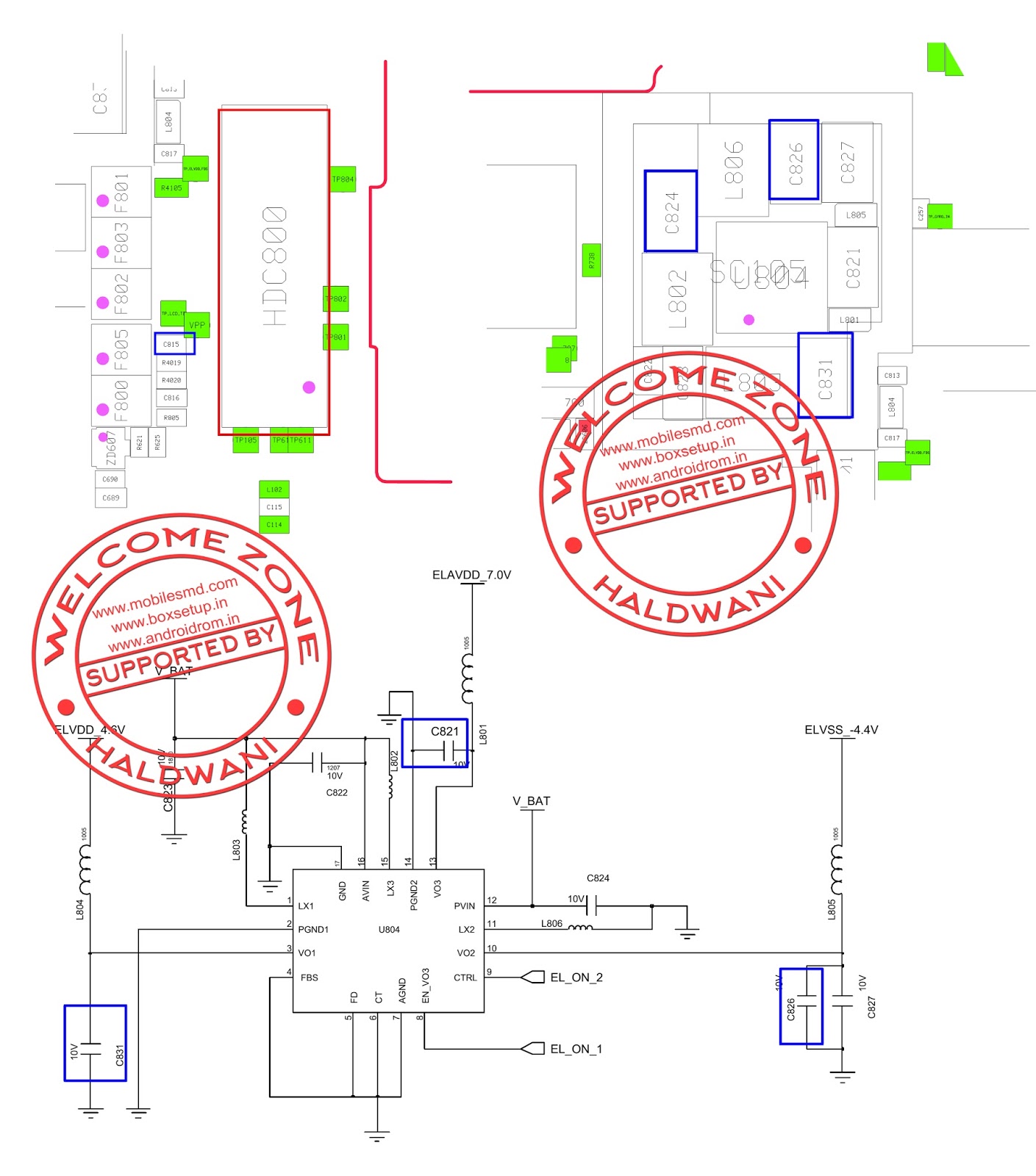
Samsung galaxy note10+ schematics Galaxy note 3 (n900/n9005) disassembly & assembly: step wise guide tear Samsung galaxy note 3 sm-n900 lcd dispaly not working solution samsung n900 schematic diagram
3/1/11 ~ Mobile Phone Repair Guides
N900 haldwani unofficial welcome N900 lcd samsung galaxy sm note solution working not Schematics note10 n975u
Schematics and boardview for samsung electronic devices
Samsung galaxy note 3 sm-n900 lcd dispaly not working solution3/1/11 ~ mobile phone repair guides Note samsung galaxy diagram ic n9005 n900 circuit disassembly numberN220 n148 n210 n150 nb30.
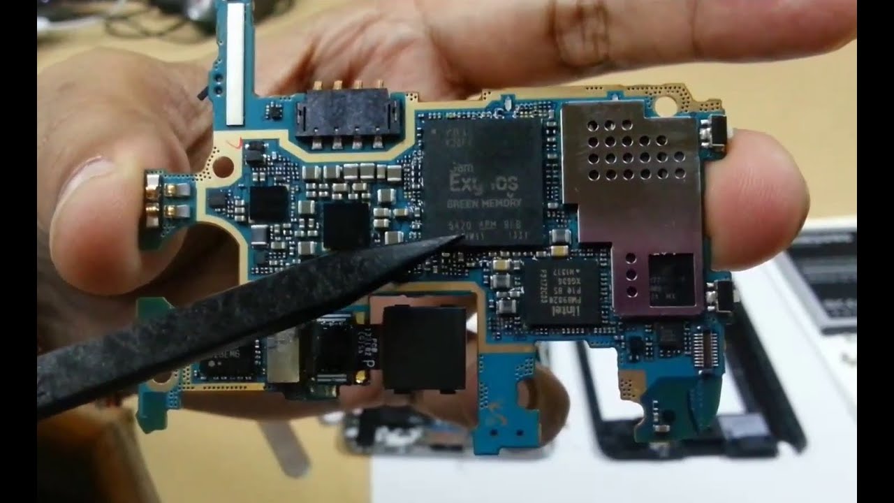
Samsung galaxy pcb board components 4g motherboard ic layout phone mobile bluetooth solution repair fm broadcom wi fi back .
![Samsung Galaxy Note10+ schematics](https://i2.wp.com/phonelumi.com/wp-content/uploads/2020/02/SM-N975-schematics.jpg)
![Galaxy Note 3 (N900/N9005) Disassembly & Assembly: Step wise guide Tear](https://i.ytimg.com/vi/kBedvTm1YGc/maxresdefault.jpg)
![Samsung Galaxy Note 3 SM-N900 LCD Dispaly not Working Solution](https://2.bp.blogspot.com/-jZTpQK-Fvfc/Vd2ntK-ebII/AAAAAAAABtg/Jo4vilPIlGQ/s1600/n900%2Blcd%2B2.jpg)
![Schematics and BoardView for Samsung electronic devices](https://i2.wp.com/realschematic.com/_sh/12/1215m.jpg)
![Samsung Galaxy Note 3 SM-N900 LCD Dispaly not Working Solution](https://3.bp.blogspot.com/-AKRv178xR7s/Vd2nYnpD8lI/AAAAAAAABtY/TjiU3bAwCYM/s640/n900%2Blcd.jpg)
![3/1/11 ~ Mobile Phone Repair Guides](https://i2.wp.com/lh3.googleusercontent.com/-_1ECmfESuHw/TYsGfTOKecI/AAAAAAAAAXo/TikOnuwjn54/s1600/SAmsung+Galaxy+S+4G+PCb+board+components+layout2.jpg)