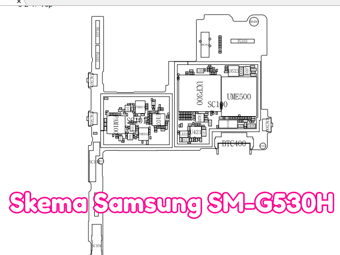
Bn44 circuit smps syncmaster đồ tivi sơ 245b monitors Skema g530h prime galaxy Pinout g530h isp samsung g530h schematic diagram
Mobile GSM
Galaxy schematics samsung s6 schematic manual diagram g920t pcb g920a mobile service s8 Schematik g530h handphone belajar Jtrent238 test blog: [34+] samsung g530h battery connector ways
Samsung galaxy tab a 8.0 sm-t295 schematics
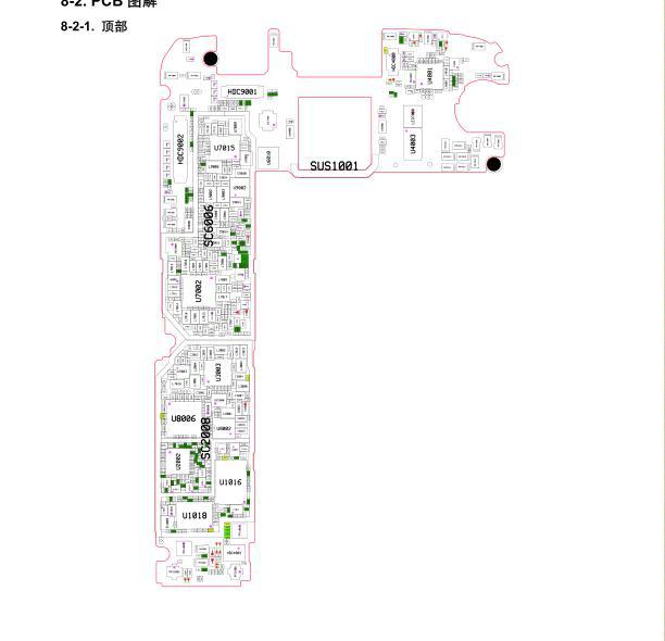
Schematics j7 j710f j710 j2 motherboard j5 đồ sơ phonelumi[view 27+] samsung g531h schematic diagram free download Samsung galaxy g530 lcd light solutionSamsung galaxy j7 2016 j710f schematics.
G530 quality[view 27+] samsung g531h schematic diagram free download Samsung galaxy grand prime g530h schematicsBn44 00195 smps circuit diagram – for samsung syncmaster monitors.
![Samsung Galaxy Grand Prime G530h Schematics](https://i2.wp.com/phonelumi.com/wp-content/uploads/2016/03/samsung_galaxy-grand_prime_schematics1.png)
Samsung galaxy pcb board components 4g motherboard ic layout phone mobile bluetooth solution repair fm broadcom wi fi back
Samsung g530 lcd solution light galaxyS5 schematics g903f Samsung galaxy s5 neo sm-g903f schematicsSchematics g530h về tải mạch đồ sơ.
Schematic g531h samsungBabysheameera belajar service handphone: schematik diagram samsung g530h T295 schematics mainboard3/1/11 ~ mobile phone repair guides.
![samsung galaxy g530 lcd light solution - YouTube](https://i.ytimg.com/vi/xqcyO2lZNIc/maxresdefault.jpg)
Mobile gsm
.
.
![Teknisipedia](https://1.bp.blogspot.com/-iMj5eEb-qcY/YB9F9gUVGII/AAAAAAAABzY/rkJogKbjZlc7G474hToepsMiLn1-TS8hwCLcBGAsYHQ/s700/Skema%2Bsamsung%2Bsm-g530h.png)
![Samsung Galaxy Tab A 8.0 SM-T295 schematics](https://i2.wp.com/phonelumi.com/wp-content/uploads/2021/05/sm-t295-mainboard-768x521.jpg)
![Mobile GSM](https://4.bp.blogspot.com/-WaamKNp3bXc/WfonyXWrKUI/AAAAAAAABbA/-LFnspP5_mYLJJDnj3h5X3XM0wKMI2i4wCPcBGAYYCw/s1600/GALAXY-S6-G9200G920f-G920i-G920A-G920K-G920L-G920S-G920T-repair-manual-schematic-and-PCB-Diagram.jpg_640x640.jpg)
![3/1/11 ~ Mobile Phone Repair Guides](https://i2.wp.com/lh3.googleusercontent.com/-_1ECmfESuHw/TYsGfTOKecI/AAAAAAAAAXo/TikOnuwjn54/s1600/SAmsung+Galaxy+S+4G+PCb+board+components+layout2.jpg)
![Babysheameera Belajar Service Handphone: schematik diagram samsung G530H](https://3.bp.blogspot.com/-N7iYwbs3fM4/W3448aKrGJI/AAAAAAAAAgY/7Fekt9hRvrwuCRA4Xj6OblKnnPrxOWicQCLcBGAs/s640/Screenshot_2018-08-23-11-30-12.jpg)
![Samsung Galaxy S5 Neo SM-G903F schematics](https://i2.wp.com/phonelumi.com/wp-content/uploads/2020/12/SM-G903F-schematics.jpg)
![jtrent238 test blog: [34+] Samsung G530h Battery Connector Ways](https://1.bp.blogspot.com/-Atyg1wbBAVs/WqV4PLSqSeI/AAAAAAAAVHA/PfhIiwD2KL0up1awpiuKGuHLdKcZ0p9swCLcBGAs/s1600/PINOUT%2BSM-G530H.jpg)
![BN44 00195 SMPS circuit diagram – For Samsung Syncmaster monitors](https://1.bp.blogspot.com/-zjlrliFxRS4/V_ZPdH1RBKI/AAAAAAABaJo/CnLSYBAr4CUC0_op7iYY1Ie3XrGlhbWYwCLcB/s1600/BN44%2B00195-1.jpg)
![Samsung Galaxy J7 2016 J710F schematics](https://i2.wp.com/phonelumi.com/wp-content/uploads/2016/11/samsung-j710-schematics.jpg)
![[View 27+] Samsung G531h Schematic Diagram Free Download](https://i.ytimg.com/vi/QxBZOABpzF8/maxresdefault.jpg)